TSMC's next-generation CoPoS packaging technology is set to enter mass production in the second half of 2028, with NVIDIA's Feynman AI chip as the likely debut customer.
Back
TSMC targets 2028 for CoPoS as NVIDIA Feynman chip nears debut
TSMC's CoPoS advanced packaging, targeting mass production in the second half of 2028, aims to solve the economics of packaging AI chips that exceed 9.5 times the standard reticle limit, according to a research report by analyst Ming-Chi Kuo.
"CoPoS is designed to improve the mass-production economics of ultra-large AI chip packaging," Kuo said in the report. The technology uses a three-layer glass core substrate — a glass core sandwiched between ABF buildup layers on both sides — with Through Glass Via fabrication, copper filling, and metallization as the key process steps.
The glass panels used in production measure 510 by 515 millimeters, which are later cut into individual glass core substrates. Kuo specifically addressed three common misconceptions: glass in CoPoS does not function as an interposer, it does not replace ABF (the two materials coexist in the stack), and chips are attached to the ABF buildup layer surface rather than directly onto glass.
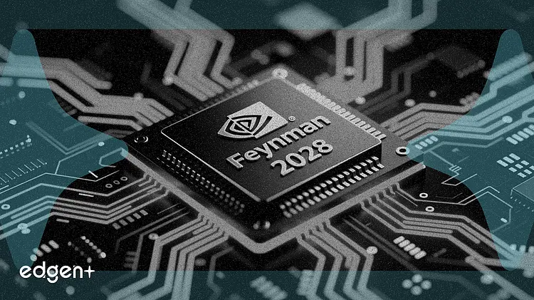
NVIDIA's next-generation Feynman architecture is positioned as the likely first CoPoS adopter, extending a partnership that already makes TSMC the sole manufacturer of NVIDIA's AI accelerators. The timing aligns with Feynman's planned launch window, though NVIDIA has not publicly confirmed the chip's packaging specifications.
CoPoS vs. the existing packaging roadmap
TSMC is simultaneously expanding its current CoWoS and SoIC platforms at an 80% and 90% compound annual growth rate, respectively, through 2027, according to the company's disclosures at its recent Technology Symposium. The foundry operates 11 advanced packaging facilities across Taiwan, including the AP7 site in Chiayi — which is expected to become its largest SoIC campus — and AP8, a converted LCD fab that could exceed 40,000 wafers per month of CoWoS capacity by late 2026.
CoPoS represents a longer-term bet on glass-based substrates for the most demanding AI workloads. While CoWoS remains the industry standard for current AI processors, chip designs are pushing beyond single-reticle limits as dies exceed 500 square millimeters — a category whose shipments are projected to grow sixfold between 2022 and 2026, per TSMC data.
Kuo expects TSMC's competitive advantage in advanced packaging to hold through at least 2032, a timeline that gives the company room to scale CoPoS alongside its N2 and A14 process nodes. TSMC is ramping N2 production at five fab phases in its first year, targeting a 70% annual capacity increase for N2 and A16 through 2028.
For investors, the CoPoS roadmap reinforces TSMC's pricing power and customer lock-in at the most advanced end of the packaging market. NVIDIA, which accounted for an estimated 15% to 20% of TSMC's 2025 revenue, gains a dedicated packaging pathway for its highest-margin products. TSMC trades at roughly 18 times forward earnings, a premium to Samsung Electronics but a discount to ASML, reflecting the market's expectation that its packaging dominance will sustain margin expansion even as Intel Foundry and Samsung Foundry attempt to close the gap.
This article is for informational purposes only and does not constitute investment advice.