
AI inference demand grew 300-fold in two years, pushing optics from the front panel to within millimeters of the compute ASIC.
AI inference demand grew 300-fold in two years, pushing optics from the front panel to within millimeters of the compute ASIC.
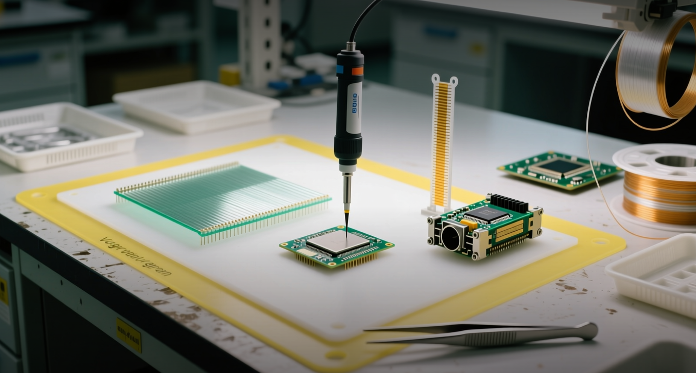
AI inference demand has grown 300-fold in two years, pushing optical interconnect from front-panel pluggable modules to co-packaged optics that sit millimeters from the switch ASIC and cut power consumption by up to 30 percent.
"The core trajectory is not simply replacing copper with fiber, but progressively moving the optical-electrical conversion point from the front panel toward the ASIC," Wang Fang, an analyst at Zhongtai Securities, said in a research note published Aug. 29.
Google's monthly token processing grew from 9.7 trillion in May 2024 to roughly 480 trillion a year later, then surpassed 3,200 trillion by May 2026. Hyperscaler capital expenditure reflects the urgency: Google raised its 2026 capex guidance to $195 billion to $205 billion, Amazon expects about $220 billion, and Meta projects $130 billion. The shift is measurable in link loss — OIF data for 112G/lane shows front-panel pluggable bump-to-bump loss of 22 to 24 dB, versus about 13 dB for near-package optics and roughly 10 dB for co-packaged optics.
The value chain is being redistributed from traditional pluggable optical modules toward high-power CW lasers, fiber array units, high-density connectivity, and advanced packaging. Nvidia has shipped two generations of co-packaged optics switches — Quantum-X800-Q3450 for InfiniBand and Spectrum-X for Ethernet — with the latter delivering 102.4 Tbps of effective bandwidth across 32 optical engines. TSMC's COUPE platform, which stacks the electronic control die directly on the photonic chip using hybrid bonding, has become the manufacturing foundation for scaling, with products entering production this year.
The physics is unforgiving. As SerDes evolves from 25G NRZ to 50G, 100G, and 200G PAM4, the effective reach of pure electrical interconnect continues to shrink. Broadcom estimates 100Gbps-per-lane DAC cables cover roughly four meters, shortening to about two meters at 200Gbps per lane; the OIF's passive copper targets for 224G/lane interfaces sit at approximately one meter. Copper's exit is not a single event but a sequential recalculation of economics across distance tiers — in-package and board-level connections span centimeters to meters, while rack-to-rack links have already gone optical.
Near-package optics (NPO) serves as the transitional platform. It deploys an independently manufacturable, testable, and replaceable optical engine adjacent to the ASIC, shortening the electrical channel while preserving component screening and yield isolation. Alibaba has adopted 3.2T NPO as a pilot starting point while advancing 6.4T UPO and interface standardization; Tencent is validating both 3.2T silicon photonics and VCSEL links in parallel; Huawei's Hi-ONE platform integrates optical engines, external light sources, connectivity, cooling, and link monitoring into a single framework.
Co-packaged optics (CPO) goes further, bringing the switching ASIC and optical engine into a shared package. Broadcom's data for a 576-GPU interconnect scenario shows DSP pluggable, linear-receive optics, and CPO consuming approximately 16.2 kW, 11.7 kW, and 7.1 kW respectively. Cisco estimates CPO reduces total system power by 25 to 30 percent versus pluggable architectures in a 51.2T system.
The migration is not a simple transfer of optical module value — it is a simultaneous restructuring of functional location, component specifications, and manufacturing responsibility. High-power CW lasers represent a relatively clear incremental opportunity: centralized light supply reduces laser count while raising per-unit power and reliability. Furukawa Electric's 8-channel external light source prototype achieves 20 dBm fiber-coupled output per channel at a 55-degree Celsius case temperature.
Fiber array units and high-density connectivity carry more universal incremental logic. Once fiber enters the high-heat-flux zone around the ASIC, it must maintain micron-level alignment under substrate warpage, thermal cycling, and vibration — driving upgrades across V-grooves, lenses, MT ferrules, MPO/MTP connectors, and blind-mate connectors. Advanced packaging, testing, and thermal management value will expand at volume production: NPO requires high-performance organic substrates and LGA sockets; CPO depends on large-format substrates, interposers, microbumps, and low-warpage materials.
TSMC's COUPE platform is emerging as the mainstream choice for CPO and optical I/O. Nvidia showcased COUPE optical engines at GTC 2025, Broadcom's future roadmap has shifted to the platform, and Ayar Labs has incorporated it into development plans. The joint yield challenge remains the core hurdle — co-packaging high-value ASICs, photonic ICs, electronic ICs, and fiber coupling structures means any single defect can amplify scrap losses. TSMC's vertical stacking approach, which uses copper-to-copper hybrid bonding to connect the electronic control chip directly on top of the optical chiplet, reduces data transmission power by up to 85 percent and shrinks electrical parasitic resistance to near zero.
For investors, the clearest beneficiaries are suppliers of CW lasers, fiber array units, precision optical components, and advanced packaging services. Marvell's data center business generated $2.17 billion in revenue in its latest quarter, up 19 percent sequentially, driven primarily by connectivity products. The company raised its fiscal 2027 revenue outlook to $12 billion and fiscal 2028 to $18 billion. But as Zhongtai's analysts caution, ultimate revenue realization still hinges on customer design wins, volume shipments, and yield data — the technology direction is clear, but the financial payoff is not yet evenly distributed.
This article is for informational purposes only and does not constitute investment advice.
